
The Silent Revolution of Advanced Materials in the Global Push for Artificial Intelligence

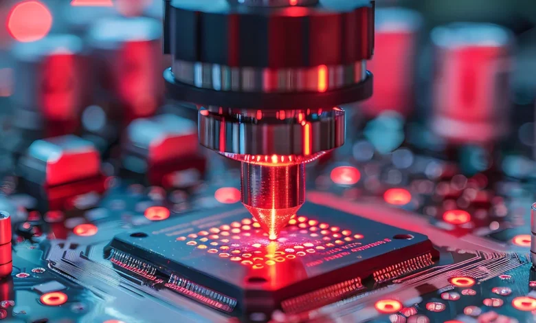
While the global discourse surrounding artificial intelligence frequently highlights the sophistication of neural networks, the massive scale of hyperscale data centers, and the soaring valuations of semiconductor giants, a more fundamental transformation is occurring at the molecular level. The rapid acceleration of AI capabilities is currently being dictated not just by code or circuit design, but by the physical limits of the materials that constitute the hardware. As the industry moves toward increasingly dense processing environments and smaller semiconductor nodes, advanced materials have transitioned from being passive components to the primary enablers—and potential bottlenecks—of technological progress.
The Physical Constraints of the AI Era
The transition from general-purpose computing to AI-centric workloads has placed unprecedented stress on physical infrastructure. Traditional computing follows a predictable cycle of logic and storage, but AI, particularly Large Language Models (LLMs), requires massive parallel processing and constant data movement. This shift demands a simultaneous increase in processing power, memory bandwidth, and energy efficiency.
In the semiconductor fabrication process, the industry is currently pushing toward the 2-nanometer (nm) node and beyond. At these scales, the behavior of atoms becomes unpredictable, and traditional materials begin to fail. For instance, the insulating layers and conductive pathways must be engineered with atomic-level precision. A single impurity or a slight instability in a chemical precursor can lead to catastrophic yield losses. Consequently, the demand for high-purity chemicals, specialized gases, and advanced photoresists has reached an all-time high.
Furthermore, the physical infrastructure of data centers is undergoing a radical redesign. The power density of an average server rack has jumped from 10–15 kilowatts (kW) to over 100 kW in AI-optimized environments. This thermal intensity renders traditional air-cooling systems obsolete, necessitating a move toward liquid cooling and advanced thermal interface materials. Without innovation in fluids and polymers that can manage this heat, the "AI revolution" would literally melt its own hardware.
A Chronology of Material Innovation in Computing
To understand the current state of the industry, one must look at the evolution of materials alongside semiconductor milestones:
- The Silicon Era (1960s–1990s): Early computing relied primarily on bulk silicon and basic polymers. Innovation was focused on refining silicon purity and developing basic lithography.
- The Strained Silicon and High-k Metal Gate Era (2000s): As transistors shrunk below 90nm, leakage became a major issue. This era saw the introduction of hafnium-based dielectrics and strained silicon to maintain performance.
- The FinFET and EUV Transition (2010s): The move to 3D transistor structures (FinFETs) required new deposition materials. The advent of Extreme Ultraviolet (EUV) lithography necessitated entirely new classes of photoresists and reflective coatings.
- The AI and Heterogeneous Integration Era (2020–Present): The current period is defined by Advanced Packaging (CoWoS), Chiplets, and High-Bandwidth Memory (HBM). These technologies require specialized adhesives, underfills, and cooling fluids that can withstand extreme thermal cycling and high-voltage architectures.
The Critical Role of Purity and Stability in Fabrication
Manufacturing a modern AI chip involves thousands of process steps, many of which occur in vacuum environments or involve aggressive chemical plasmas. In these settings, the materials used to build and seal the equipment are as critical as the silicon itself.
Perfluoroelastomers (FFKMs) are a prime example. These high-performance seals must maintain their integrity while exposed to reactive gases and temperatures exceeding 300°C. Any degradation of the seal releases microscopic particles into the cleanroom environment, which can ruin an entire batch of wafers. Industry leaders like Syensqo are now focusing on the next generation of these materials, moving toward fluorosurfactant-free manufacturing processes to meet both performance demands and increasing environmental regulations.
According to market data, the semiconductor materials market is projected to exceed $75 billion by 2027, driven largely by the specialized requirements of AI-grade chips. The margin for error has shrunk to the point where "high purity" now often refers to parts-per-trillion (ppt) levels of contamination, a standard that requires sophisticated chemical engineering and supply chain control.
Thermal Management and the Data Center Overhaul
As AI workloads migrate from training labs to global deployment, the energy footprint of data centers has become a primary concern for tech giants like Google, Microsoft, and Amazon. The International Energy Agency (IEA) estimates that data center electricity consumption could double by 2026, reaching over 1,000 terawatt-hours (TWh)—roughly equivalent to the total electricity consumption of Japan.
A significant portion of this energy is used not for computation, but for cooling. This has triggered a shift in data center architecture:
- Direct-to-Chip Cooling: Specialized fluids are circulated through cold plates directly attached to the processors.
- Immersion Cooling: Entire servers are submerged in non-conductive dielectric fluids.
- High-Voltage Power Delivery: To reduce resistive losses, data centers are shifting to higher voltage architectures (e.g., 48V instead of 12V), requiring new insulating materials that can prevent electrical arcing in cramped spaces.
Materials science companies are adapting knowledge from the electric vehicle (EV) sector to solve these problems. The cooling systems in a high-performance EV battery share many characteristics with the thermal management needs of an AI server farm. By repurposing specialized coolants and high-voltage polymers, manufacturers are accelerating the deployment of more efficient AI infrastructure.
The Paradox: Using AI to Discover AI Materials
One of the most significant shifts in the industry is the application of AI to the field of materials science—a discipline traditionally characterized by slow, iterative "trial and error" experimentation. The development of a new polymer or specialty fluid can traditionally take five to ten years from laboratory discovery to commercial qualification.
To keep pace with the 18-month cycles of the semiconductor industry, materials companies are deploying "Materials Informatics." This involves using machine learning models to predict the properties of molecular structures before they are synthesized in a lab.
Syensqo, for instance, has integrated the Microsoft Discovery platform into its research and development workflow. This AI-driven tool allows researchers to screen thousands of molecular candidates for heat transfer fluids and lubricants in a fraction of the time it would take through physical testing. By identifying the most promising candidates early, scientists can focus their efforts on refining materials that are most likely to meet the rigorous qualification standards of semiconductor manufacturers.
This creates a virtuous cycle: AI tools accelerate the discovery of advanced materials, which in turn enable the production of more powerful AI chips, which then provide the computing power to run even more sophisticated material discovery simulations.
Sustainability and the Evolving Definition of Performance
In the modern industrial landscape, "performance" is no longer measured solely by technical specifications. Regulatory pressure and corporate social responsibility have integrated sustainability into the core requirements of material science.
The semiconductor industry is currently navigating a complex regulatory environment regarding Per- and Polyfluoroalkyl Substances (PFAS), often referred to as "forever chemicals." While these materials are essential for chip manufacturing due to their unique chemical resistance, there is a global push to find safer alternatives or more responsible manufacturing methods.
The industry’s response has been to innovate rather than retreat. The development of fluorosurfactant-free perfluoroelastomers demonstrates that it is possible to maintain—and even improve—material performance while reducing environmental impact. For semiconductor manufacturers, this transition is not optional; as global regulations like the EU’s REACH tighten, the long-term viability of their supply chains depends on the availability of "green" advanced materials.
Broader Implications and Market Analysis
The reliance on advanced materials has profound geopolitical and economic implications. As nations race to secure semiconductor sovereignty through initiatives like the U.S. CHIPS Act and the European Chips Act, the focus is often on the "fabs" (fabrication plants). However, a fab is useless without a steady supply of advanced chemicals and materials.
Market analysts suggest that the next phase of the "AI arms race" will be won by those who control the material supply chain. This includes the rare earth elements used in high-performance magnets for cooling fans, the specialized gases used in etching, and the proprietary polymers used in advanced packaging.
Furthermore, the shift toward advanced packaging—where multiple chips are stacked together—represents the next frontier. This "More than Moore" approach relies entirely on material innovation to manage the structural integrity and heat dissipation of stacked components. If materials science cannot solve the bonding and thermal issues of 3D-stacked chips, the industry will hit a performance wall that no amount of software optimization can overcome.
Conclusion: The Earned Progress of the AI Future
The narrative of artificial intelligence is often told through the lens of intangible data and ethereal algorithms. Yet, the reality of AI is deeply rooted in the physical world. Every calculation performed by a generative AI model is the result of electrons moving through a complex architecture of silicon, metal, and specialized polymers.
Progress in this field is not a given; it is earned through rigorous engineering and the constant pushing of physical limits. As AI technology continues to evolve, the materials that support it must become more durable, more pure, and more efficient. The companies that can master the chemistry of these components will be the ones that define the boundaries of what artificial intelligence can eventually achieve. In the end, the future of AI will be written not just in code, but in the very atoms that make computing possible.