
The Material Foundation of Artificial Intelligence How Advanced Chemistry Enables the Next Era of Computing Performance

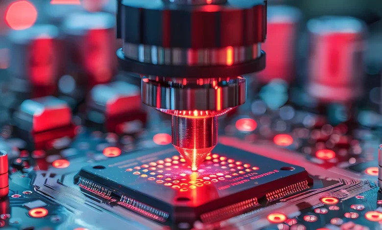
While the global discourse surrounding artificial intelligence frequently highlights the sophistication of Large Language Models, the geopolitical race for high-end GPUs, and the multi-billion-dollar investments in hyperscale data centers, a more fundamental revolution is occurring at the molecular level. Beneath the layers of code and neural networks lies a physical infrastructure defined by advanced materials science. As the semiconductor industry pushes toward the physical limits of silicon, the materials that house, cool, and connect these systems have transitioned from passive components to the primary gatekeepers of technological progress.
The current trajectory of AI development is predicated on an insatiable demand for processing power, memory density, and energy efficiency. However, every incremental gain in computing performance imposes escalating physical demands on the hardware. High-performance computing (HPC) environments now operate under thermal and chemical stresses that would have been untenable a decade ago. To sustain this momentum, the industry is increasingly turning to specialty chemicals, high-performance polymers, and innovative thermal management fluids to bridge the gap between theoretical architectural designs and functional, reliable hardware.
The Shift from Architecture to Materiality
For decades, the primary driver of computing progress was the refinement of chip architecture and the shrinking of transistors, famously described by Moore’s Law. However, as transistor gates approach the size of a few atoms, the challenges of leakage, heat dissipation, and manufacturing precision have become insurmountable through design alone. Today, the manufacturing of a single state-of-the-art semiconductor chip involves thousands of precision-controlled steps where the margin for error is virtually nonexistent.
In these hyper-sensitive environments, the stability of the materials used in the fabrication process is paramount. Micro-variations in chemical purity or the thermal expansion of a seal can lead to catastrophic yield losses. Consequently, materials companies like Syensqo are developing a new generation of elastomers and polymers designed to withstand aggressive plasma etching and highly reactive chemical cleaning cycles. These materials must maintain their integrity at extreme temperatures and under vacuum conditions that would degrade standard industrial components.
The evolution of the semiconductor market, which is projected to reach a valuation of $1 trillion by 2030 according to McKinsey & Company, is now tethered to these material innovations. Without advanced polymers that can ensure high-purity environments, the transition to sub-3nm process nodes would be physically impossible.
A Chronology of Material Innovation in Computing
The role of materials in computing has evolved through several distinct eras, each marked by a specific challenge that required a chemical solution:
- The Silicon Era (1960s–1990s): The focus was primarily on the purity of bulk silicon and the development of basic photoresists for lithography. Material science was a supporting discipline to electrical engineering.
- The Interconnect Challenge (2000s): As chips became faster, traditional aluminum wiring hit a "resistance-capacitance" wall. The industry shifted to copper interconnects and low-k dielectrics, a transition that required entirely new chemical mechanical planarization (CMP) slurries and barrier materials.
- The Thermal Wall (2010s): The rise of mobile computing and early cloud data centers made heat the primary enemy. This era saw the introduction of advanced thermal interface materials (TIMs) and the first widespread use of specialty plastics in mobile device housing for heat dissipation.
- The AI and Infrastructure Era (2020s–Present): The current era is defined by extreme power density. AI chips like the NVIDIA H100 series consume significantly more power than their predecessors, necessitating a shift from air cooling to liquid cooling and the adoption of high-voltage power architectures.
The Data Center Transformation: From Air to Liquid
The physical infrastructure of the data center is undergoing its most significant transformation since the invention of the rack. As AI workloads increase, the heat generated by dense GPU clusters is exceeding the capacity of traditional air-cooling systems. According to the International Energy Agency (IEA), data centers currently account for approximately 1% to 1.5% of global electricity use, a figure expected to rise sharply as AI deployment scales.
To combat this, the industry is pivoting toward direct-to-chip liquid cooling and immersion cooling. These systems rely on specialty fluids that must possess a unique combination of properties: high thermal conductivity, low viscosity, and absolute dielectric stability to prevent electrical shorts. Syensqo and other leaders in the specialty chemical sector are adapting technologies originally developed for the automotive and aerospace industries to meet these needs.
There is a notable parallel between the evolution of AI data centers and the development of electric vehicles (EVs). Both require high-voltage power architectures to minimize energy loss during transmission and sophisticated thermal management systems to protect sensitive electronics. By leveraging fluid-circulation expertise from automotive coolant systems, materials scientists are accelerating the deployment of next-generation cooling for AI servers. This cross-pollination of industries is shortening the R&D cycle for data center infrastructure, which is under pressure to keep pace with the six-month to one-year release cycles of new AI chips.
Redefining Performance through Sustainability
While technical specifications like thermal resistance and chemical purity remain the primary metrics for success, the definition of "performance" is expanding to include environmental responsibility. The semiconductor and data center industries are under increasing scrutiny regarding their carbon footprint and the chemical lifecycle of their components.
A critical area of focus is the use of perfluoroelastomers (FFKMs), which are essential for sealing semiconductor manufacturing equipment. These materials are prized for their ability to withstand the harshest environments on earth. However, traditional manufacturing processes for these materials have often relied on fluorosurfactants, which are subject to tightening global regulations.
In response, the industry is moving toward "fluorosurfactant-free" manufacturing processes. Syensqo’s development of a new generation of perfluoroelastomers that do not compromise on performance while utilizing more responsible production methods represents a significant milestone. This shift indicates that the future of materials science is not just about doing more, but about doing it with a lower environmental impact. This is not merely a corporate social responsibility initiative; it is a business necessity, as regulatory frameworks like the EU’s REACH (Registration, Evaluation, Authorisation and Restriction of Chemicals) continue to evolve.
Accelerating Discovery: AI as Both Tool and Target
Perhaps the most meta-physical aspect of the current materials revolution is the use of AI to discover the very materials that will power future AI. Historically, discovering a new specialty molecule or polymer was a process of "Edisonian" trial and error that could take decades. Researchers would synthesize a compound, test it, observe the failure, and iterate.
Today, materials scientists are utilizing AI-driven platforms, such as the Microsoft Discovery platform, to simulate the properties of thousands of molecular candidates in a digital environment. By using "in silico" testing, researchers can predict how a new heat-transfer fluid will behave under specific pressures and temperatures before a single drop is synthesized in a lab.
This AI-accelerated discovery process is particularly vital for developing next-generation heat transfer fluids. By identifying the most promising molecular structures early, companies can focus their laboratory resources on the candidates with the highest probability of success. This reduces the time-to-market for critical infrastructure components, allowing material innovation to finally match the "warp speed" of software development.
Analysis of Implications: The Material Bottleneck
The reliance on advanced materials introduces a new set of strategic implications for the global technology supply chain. As AI performance becomes increasingly dependent on specialty chemistry, the following trends are likely to emerge:
- Supply Chain Concentration: The production of high-performance polymers and specialty fluids is concentrated among a few global players with the R&D capacity to innovate at this level. This creates a new "chokepoint" in the AI supply chain, parallel to the concentration of high-end chip manufacturing at TSMC.
- Cost Sensitivity: While the cost of a seal or a liter of coolant is a fraction of the cost of a GPU, the failure of these materials can result in the loss of millions of dollars in hardware or downtime. Therefore, "premium" materials will command a higher share of the data center CAPEX (Capital Expenditure).
- Regulatory Risk: The industry’s dependence on fluorinated chemistry remains a point of vulnerability. Ongoing innovation in "green chemistry" will be the only way to mitigate the risk of sudden regulatory bans on essential materials.
Conclusion: Progress is Earned at the Atomic Scale
The future of artificial intelligence is often depicted as a digital ether—a world of intangible data and ethereal algorithms. In reality, AI is a heavy industry. It is an industry of silicon, copper, high-performance polymers, and sophisticated fluids.
As we look toward the next generation of computing, it is clear that progress is not guaranteed by better code alone. It is earned through the rigorous application of chemistry and physics. Every leap in AI capability requires a corresponding leap in the physical endurance of the systems that support it. For the companies at the forefront of materials science, the challenge is to continue redefining the limits of the possible, ensuring that the atoms can keep up with the bits. The next breakthrough in AI may not come from a software lab in Silicon Valley, but from a chemical laboratory where the next great molecule is being synthesized.