

The Evolution of Cloud-Based Silicon Engineering
Historically, the semiconductor industry relied on fixed, on-premise x86 server clusters to manage EDA workloads. This model often required companies to size their data centers for peak demand, leading to prolonged periods of costly underutilization. The transition to cloud-based EDA on Microsoft Azure has fundamentally altered this paradigm, introducing the flexibility to scale compute resources up or down based on the lifecycle of a silicon project.
The shift to Arm-based custom silicon, specifically the Cobalt line, represents a strategic move by Microsoft to optimize its infrastructure for the unique requirements of high-performance computing. Silicon engineering teams at Microsoft are now leveraging Cobalt-based virtual machine (VM) instances to streamline the development of increasingly sophisticated chips intended for the company’s cloud data centers. This internal utilization acts as a proof-of-concept for the broader Azure customer base, proving that specialized compute hardware can provide a distinct competitive advantage in the race to design complex, next-generation AI and server silicon.

Architecture Designed for Throughput
The core challenge in EDA is the diversity of compute requirements. Different stages of the design process, from RTL simulation to static timing analysis, place unique demands on a processor’s architecture. CAD managers, who oversee these large-scale environments, prioritize predictable per-core performance, especially during high-concurrency overnight regressions.
The Cobalt 200 architecture addresses these bottlenecks through several design choices. It moves away from the overhead of hyperthreading, opting instead for a configuration that features dedicated physical cores. Each core is equipped with a 3MB L2 cache, complemented by high-provisioned memory bandwidth. This combination ensures that even under the intense pressure of verification farms running at maximum capacity, the platform maintains robust throughput. Because the tools—including industry standards from Cadence, Synopsys, and Siemens—were already enabled on Cobalt 100, the transition to Cobalt 200 required no modifications to the underlying software stack, allowing engineers to focus entirely on measuring performance gains.
Empirical Performance Benchmarks
To evaluate the efficacy of the Cobalt 200, Microsoft tested a variety of workloads spanning the standard silicon development flow. These tests compared job completion times against both the Cobalt 100 and a selection of established x86 Azure virtual machines.
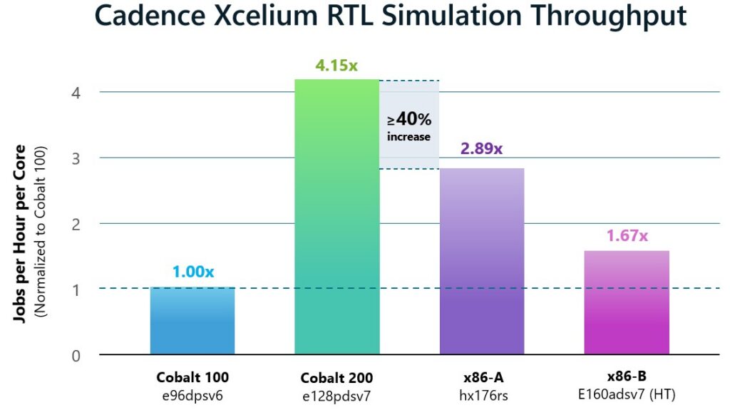
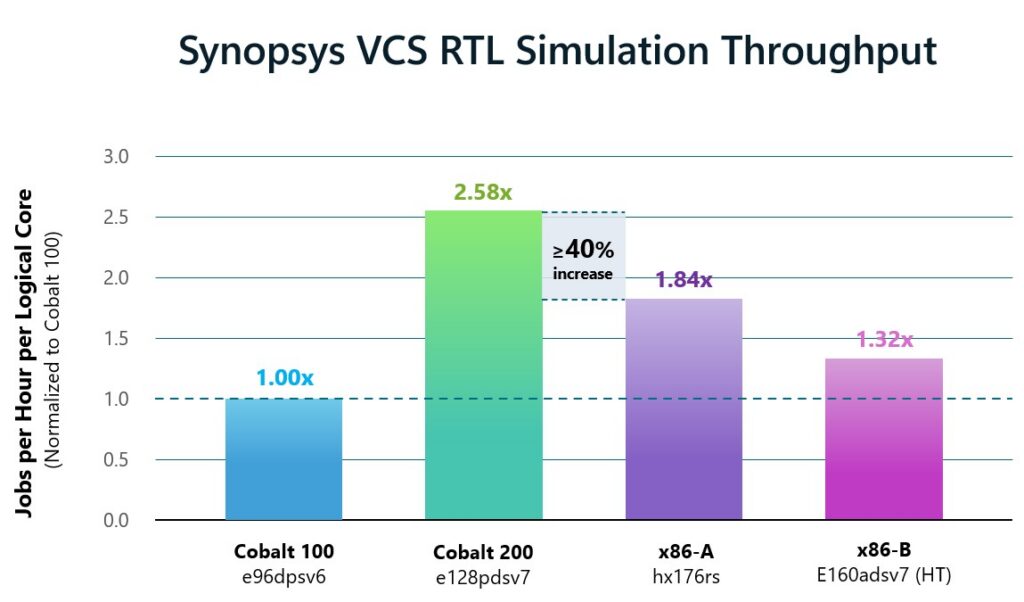
In the realm of digital simulation, which utilizes tools such as Cadence Xcelium and Synopsys VCS, the Cobalt 200 demonstrated a substantial lead. These tools are the workhorses of functional verification, where RTL simulation consumes the majority of available compute resources. Testing revealed that the Cobalt 200 delivered more than 40% higher throughput per logical core than any other tested system, including the prior generation.
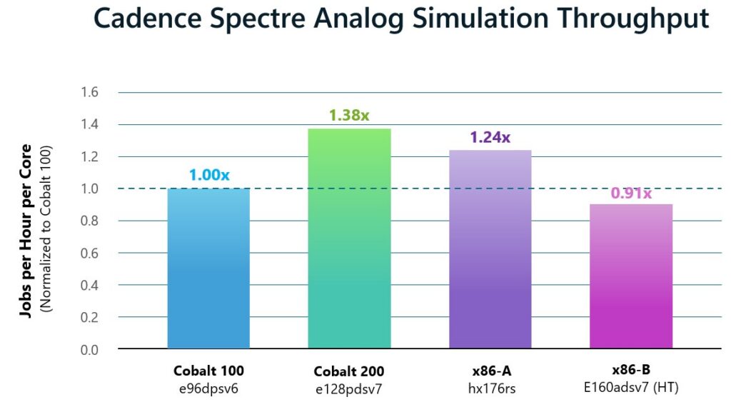
For analog and mixed-signal simulation—a process dominated by multithreaded performance and managed via Cadence Spectre—the Cobalt 200 achieved 38% higher throughput per logical core compared to the Cobalt 100, and it outperformed all evaluated x86-based configurations by margins of 11% to 52%.
Physical verification, specifically the Design Rule Checking (DRC) processes performed by Siemens Calibre, also saw a marked improvement. In tests using an IP Macro with 16 cores per job, the Cobalt 200 reduced wall time by approximately 23% compared to the Cobalt 100, translating to a 1.30x performance improvement. Finally, in static timing analysis—where teams use Synopsys PrimeTime to ensure a design meets strict operational requirements—the Cobalt 200 doubled the peak throughput per logical core compared to the Cobalt 100, while again surpassing the performance of comparable x86 Azure VMs.
Industry Perspectives and Partnerships
The results have drawn praise from the EDA industry, which views the collaboration as a vital development in addressing the widening complexity gap in semiconductor design. Paul Cunningham, Senior Vice President and General Manager of the System Verification Group at Cadence, noted that the qualification of Cadence EDA workflows on Cobalt 200 provides semiconductor teams with the necessary flexibility to scale compute for demanding verification cycles.
Similarly, Craig Johnson, Vice President of Cloud Solutions at Siemens EDA, highlighted the importance of matching workload-specific requirements to appropriate compute architectures. From the perspective of Synopsys, Sanjay Bali, Senior Vice President of EDA Product Management and Strategy, emphasized the significance of the 40% faster runtimes observed with VCS and the 2x per-core throughput with PrimeTime, noting that these improvements are essential for the development of next-generation AI silicon.
The Virtuous Cycle of Silicon Development
The relationship between Cobalt 200 and the tools used to create it represents a "virtuous cycle." The EDA tools themselves were instrumental in designing the Cobalt 200 chip; now, that chip is accelerating the design of future Cobalt products. By monitoring how these workloads behave at scale on the new architecture, Microsoft gains telemetry that informs the design of future Azure compute infrastructure. This recursive process ensures that each generation of hardware is more tailored to the specific software requirements of the next, effectively shortening the development timeline for new custom processors.
Implications for the Semiconductor Industry
The broader implication of these results is the potential for a fundamental shift in how the industry approaches silicon development costs. By providing a platform that exhibits both higher per-core throughput and superior scaling, Azure is offering a solution that could reduce the time-to-market for complex chip designs. The fact that these performance gains are realized without requiring code refactoring for existing EDA software lowers the barrier to entry for teams looking to migrate their design environments to the cloud.
As Azure Cobalt 200 moves toward general availability, Microsoft’s focus is shifting toward broader workload coverage and testing at an even greater scale. The company is currently working with its EDA partners to further tune software performance on the platform. For engineering organizations currently evaluating their own transition to cloud-based infrastructure, the data suggests that the Cobalt 200 is not merely an incremental upgrade, but a highly specialized tool designed to meet the rigorous demands of modern silicon engineering. With the combination of enhanced cache structures, improved memory bandwidth, and the elimination of hyperthreading overhead, the platform provides a compelling case for the necessity of workload-optimized silicon in the future of the data center.